From Simple to Complex PCB Designs
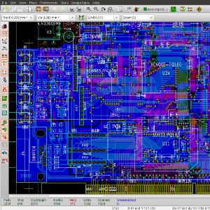
Designing electronic services and products in the UK, we are able to undertake a wide range of PCB layout tasks, from simple double sided through hole PCB artwork taking a few hours to complete to over 10 layer high-density PCBs for demanding applications such as high speed digital and wireless technology designs.
As experienced and highly skilled Electronic Design Engineers we have a deep understanding of how to get the best from a PCB design, circuitry and technology employed. When laying out a PCB from a customer’s schematic, in addition to producing high-quality PCB artwork, we are able to make helpful suggestions or flag up issues with the circuitry, something regular PCB CAD layout technicians are unable to do. If requested, we can get more involved with your circuit design, including helpful design reviews over the phone, at a location of your choice or here at Milliamp Technologies in Lancaster, United Kingdom near the beautiful Lake District. Alternatively, we can just get on with things and “work to specification” as PCB layout subcontractors if this is preferred.
For the most demanding technology designs, we are also able to undertake impedance controlled PCB layout, with full design and PCB build-up calculations available for submission to the manufacturer to allow trouble free impedance controlled production and test. For peace of mind for the most sensitive hi-specification impedance controlled PCB artwork we also recommend we perform verification by computer based PCB Signal Integrity (SI) analysis tools, which allows us to prove by simulation that a board is operating within its planned design parameters, such as trace impedance, signal flight time, noise, crosstalk and simulated EMC emissions. It is not possible to evaluate these parameters in the lab easily without building a prototype and testing with expensive instruments. Simulation helps avoid lab testing time and expensive board re-spins as we can be confident of exactly how a PCB layout performs before it has even been made !
Our PCB Layout services include:
- Use of PCB Layout tools to suit you – we are able to layout PCBs a variety of CAD, EDA and PCB design software tools including Altium Designer/Protel 99, Labcenter Proteus, Autodesk Eagle, RS Design Spark PCB, EasyPC, Mentor PADS & KiCad and many others. We are more than happy to work with any PCB tool our customers require.
- New or continue existing PCB layouts – we are able to start a PCB layout from scratch or continue an ongoing design supplied in a variety of formats, either from schematics supplied from customers or from our own schematics if you have asked us to do this also as part of our Electronic Circuit Design services.
- 2 layer PCBs to complex impedance controlled 10+ layer board layout – we can use a variety of layout approaches to suit the design, including 100% auto-routed PCB to keep costs down to manual routing for critical hi-specification designs. We develop our PCB designs compliant to IPC guidelines and standards.
- PCB manufacturing data generation – RS-274X gerbers, Excellon drill data, XY centroid (pick & place) data and IPC-D-356 netlists. Board stackup and material specification documentation also provided. We can optionally work to IPC-2581. Fully documented which can further be developed into a Manufacturing Data Pack (MDP) as part of our Pre-Production Engineering Services.
- “Front End” gerber work – for gerber modifications, DRC checks, panelisation etc. as part of our Pre-Production Engineering Services.
- Board level Signal Integrity – (SI) simulation quickly identify any issues such as crosstalk, signal degradation, noise and other unwanted effects that may be present due to electromagnetic interference or coupling on the PCB.
- 3D PCB modelling – that can be used for mechanical assembly verification and integration with other CAD systems.
With the outputs from our PCB Artwork layout activities, we are able to produce a PCB prototype if required as part of our Product Prototyping service.
Variety of PCB Types
We have a variety of experience in PCB design types including:
- Multilayer Impedance Controlled PCBs.
- PCB antennas and RF.
- High Voltage PCB design.
- Rigid, Flexible and Semi-Flexible PCBs.
- Thermally optimised boards with Insulated Metal Substrate PCB (aka T-Clad).
- Specialist designs including ceramic PCBs.
